
10min read
Historical Background
The beginning of the development of a Swiss quartz system for wrist watches must be credited to three different approaches, listed chronologically below:
The first starting to look at quartz for integrating it as an oscillator for wrist watch calibers was Battelle in Geneva. This American institution specialised in microelectronics was commissioned by Omega to find a technical solution for competing against the rise of electro-mechanical and electro-magnetic systems. After a meta-analysis of the existing developments, Battelle suggested to look into the miniaturisation of the quartz system starting from 1957. The development within Battelle for Omega will be discussed separately.
The second approach into the miniaturisation of the quartz system for wrist watches was done by Longines which contacted Golay SA in Lausanne in August 1964 to partner for the development of a first marine chronometers sized quartz system, which will be gradually miniaturised to reach wrist watch size. The development within Golay and Longines will also be discussed in a dedicated subsection.
The third approach was made by the Centre Electronique Horloger (CEH) in Neuchâtel. The CEH started as a conglomerate of Swiss watch and parts manufacturers for competing mostly against the very successful ‘Accutron‘ system and thus investing at first in the development of a reliable electro-magnetic systems. The first mentioning of a quartz regulator at the CEH appears in an internal report in February 1965, when Armin Frei proposed a system with two low frequency quartz bars. Later, thanks to engineer Armin Frei and the director of the CEH, Roger Wellinger, the initial strategy optimising tuning fork systems was turned around in November 1965 to consecrate most research efforts towards the development of a quartz regulator system for wrist watches. The developments at the CEH are discussed in a specific section with corresponding subsections.
All approaches will be done independently from each other, even if Longines and Omega took part in the development of the calibers at the CEH. Not only will all the three mentioned approaches be successful, each approach will generate a different solution for the quartz miniaturisation. Of all Swiss and also international efforts for the development of a wrist watch sized quartz watch the CEH will be the first to present a working prototype, named Beta 1, in July 1967.
Technological Features
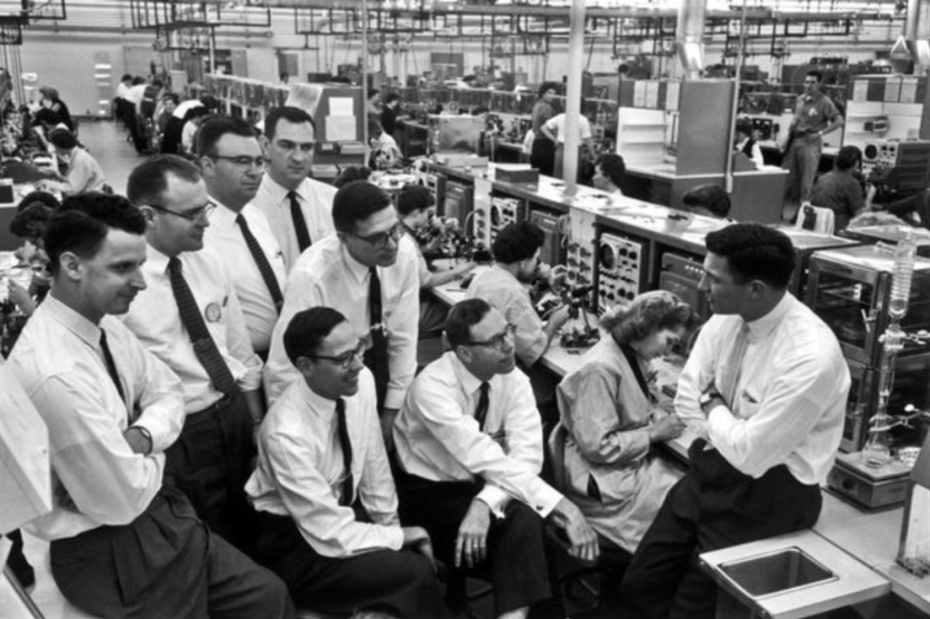
The technology for the development of a wrist watch sized quartz caliber is quite straight forward, if analysed in view of the technology available today. During the mit 1950s up to the end of the 1960s, several, colossal, technological feats have impeded the speedy development of a suitable quartz system small enough to be worn at the wrist.
The theoretical concept for such a development is easy: needing a quartz oscillator, an electronic circuitry controlling the oscillations of the quartz and dividing the oscillations plus a transduction of this divided frequency into circular motion through a motor and a wheel system to drive the hands. Not to forget, that also a very small battery alimenting it all and housed inside the wrist watch case is crucial. Even Max Hetzel, the inventor of the electro-magnetic ‘Accutron‘ system, was aware since the early 1960s, that such a quartz system would be superior, concerning precision, to all other battery driven or mechanical systems. What Hetzel predicted though, was that the technology to solve the equation to fit all required features plus a battery into a wrist watch sized case would be impossible. This is the reason, why Hetzel refused to work on the development of a quartz. The main technological problems were the following:
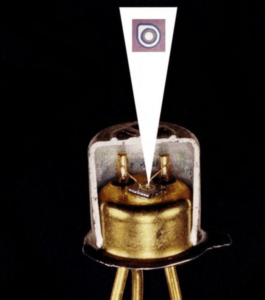
Quartz oscillator: The miniaturised quartz oscillator as regulator organ of the watch must be suspended in a vacuumed shell. Apart of the immensely small crystal and the precise cutting of such miniature crystal, the suspension and the perpetual vacuum must be ensured and must resist daily wear. Finding the ideal shape and cutting of the quartz crystal itself represented months of calculations. The research of facilities able to comply with the needed requirements to build and house such a small quartz was no easy task either. While the CEH and Golay SA opted for a crystal in rectangular bar shape, Battelle went for a lenticular quartz crystal, whereas the Japanese Seiko will use tuning fork shaped crystals.
Electronic circuitry: The electronic, integrated circuitry was non-existing in the mid 1950s. The miniaturised germanium transistors for use in radio devices were the top of the available technology. Apart of the miniaturisation of transistors, such as the germanium transistor used in the early ‘Accutrons‘, one of the revolutionary developments concerning the further miniaturisation of electric devices, permitting their integration into wrist watches, was made in America at the end of the 1950s. Especially the company Fairchild co-founded by the young Swiss engineer Jean Hoerni would set one important mark for the electronic revolution. Hoerni invented the ‘planar process’ to manufacture two dimensional circuits on silicon wafers and patented this in 1959 (1).
This process is called ‘planar process’ because it allows to produce stable device structures through a sequence of steps carried out on the surface plane of a thin silicon crystal. One historian has called Hoerni’s invention (1):
“the most important innovation in the history of the semiconductor industry.”

A thin silicon (Si) wafer is coated with Silicon Oxide (SiO2). The circuit pattern is etched onto such silicon wafer by means of photolithographic (photoengraving) process. To do so, the silicon oxide surface is coated with a photosensitive polymer applied through a photographic mask (a), leaving the pattern of the future circuitry blank. The polymer pattern protects selected oxide regions on the silicon surface when it is immersed in a hydrofluoric acid bath or exposed to gas phase etchants, which then forms a surface consisting of windows exposing the silicon underneath the silicon dioxide layer (b). Silicon itself is a poor conductor, so impurities are introduced (dopant atoms) inside the silicon windows (c). Through the windows the impurities diffuse into the silicon and to render it more conductive (d). A linear network of conductive pathways inside the silicon wafer has been formed. This principle has been used the first time to produce the Fairchild 2N1613 transistor (1, 2, 5).
The principles of the ‘integrated circuit’ had been invented before, by Jack Kilby at Texas Instruments in 1958, but the system invented by Kilby on germanium and not silicon was flawed and could not be mass produced. Hoerni’s ‘planar process’ allowed for the development and industrial manufacturing of highly reliable miniature bipolar -and later towards 1963 the more powerful MOS (unipolar, less energy draining) transistors (electrical switches). These elements were later combined to more complex microchips, which contain many miniature transistors, diodes, capacitors, resistors and even an occasional inductor (1, 3).
The first integrated circuits on silicon were developed by Fairchild under the supervision of Robert Noyce, just a few months after the development of the planar process. They were relatively slow, replaced only a handful of components, and sold for many times the price of their discrete transistor counterparts. This was the reason for the Swiss to either develop the technology themselves or use discrete elements. The former path was taken by the CEH who later took Faselec on board to optimise their own bi-polar technology, initially developed for the use in tuning fork systems, for the new application in quartz regulated watches, the latter path was used by Longines for the circuitry of their cal.: 6512 which will be running the ‘Ultra-Quartz’ model (4). The more powerful MOS technology was used by Battelle for Omega in their development of the predecessor of what will be marketed by Omega as the ‘Megaquartz 2.4MHz’ model. Later, towards 1967, the ‘ion implantation process’ will allow for the industrial and high scale production of reliable, low energy CMOS integrated circuits for the integration into the development of wrist watch sized quartz movements. It is then, that Jean Hoerni will leave Fairchild to create Intersil, which will specialise in the production of such low energy, CMOS IC’s. The CEH will be able to produce their own CMOS IC’s per 1971 (8).
MOS vs. CMOS Integrated Circuits
MOS (Metal-Oxide-Semiconductor) and CMOS (Complementary Metal-Oxide-Semiconductor) are two types of integrated circuit technologies that are widely used in modern electronics. Here are the key differences between CMOS and MOS circuits (9):
Basic Technology: MOS technology is used to implement electronic components on silicon substrates. CMOS, on the other hand is a specific, more elaborated type of MOS technology.
Transistor Types: MOS circuits use either p-type or n-type MOS transistors, while CMOS circuits use a combination of both p-type and n-type MOS transistors. In CMOS technology, complementary pairs of p-type and n-type transistors are used to achieve low power consumption and high noise immunity.
Power Consumption: CMOS circuits generally consume less power compared to MOS circuits. This is because CMOS circuits have low static power dissipation due to the fact that one type of transistor is off when the other is on.
Noise Immunity: CMOS circuits have better noise immunity compared to MOS circuits. This is because CMOS circuits use complementary pairs of transistors that switch between high and low states, which helps in reducing noise susceptibility.
Speed: In general, CMOS circuits are slower than MOS circuits. This is because the presence of both p-type and n-type transistors in CMOS circuits can introduce additional delays due to the need to switch between the two types of transistors.
Applications: CMOS technology is widely used in digital logic circuits, microprocessors, memory chips, and other digital integrated circuits due to its low power consumption and noise immunity. MOS technology is used in various analog and digital applications, but it is not as common in modern integrated circuits as CMOS technology.
Overall, CMOS circuits offer advantages in terms of power consumption and noise immunity compared to traditional MOS circuits, making them the preferred choice for many modern electronic applications, also electronic watches (9).
Battery: Already LIP in Besançon had considerable problems finding adequate batteries for driving their R27 caliber electro-mechanical prototypes in 1954. The first manufacturers seeing a future market in miniaturised batteries and thus researching the problem were Leclanché in Switzerland and Mallory in the USA. Latter brand started producing mercury batteries for portable electronic devices during WWII. In 1964 they registered their trademark ‘Duracell’ and began rebranding under the new name with the intent of marketing directly to consumers instead of industrial and military customers (6).
Ref.:
- Computerhistory.org – 1959
- Electronics Tutorial
- Tutorialspoint
- Computerhistory.org – 1962
- The Transistor Museum
- Wikipedia
- Computerhistory.org – 1960
- Personal communication with a former Executive Vice-President of Ebauches SA, in charge of Research & Engineering.
- Quora
